- Hearing Aid
- Amplified Ear
- A Low Cost Hearing Aid
- Studio Series Stereo Headphone Amplifier
- Stereo Headphone Amplifier Circuit Schematic
- Pure Class-A Headphone Amplifier Schematic
- Portable Headphone Amplifier Circuit
- A Hiqh Quality Headphone Amplifier Schematic
- Ultra-High Fidelity High Power Amplifier Reference Design
- Speach Amplifier
- DC-Coupled Audio Amplifier
- A Low Power Wireless Audio Power Amplifier
- 8 Watt Audio Power Amplifier Schematic
- 7 Watt Audio Power Amplifier Circuit Schematic
- 60 Watt Audio Power Amplifier Circuit Diagram
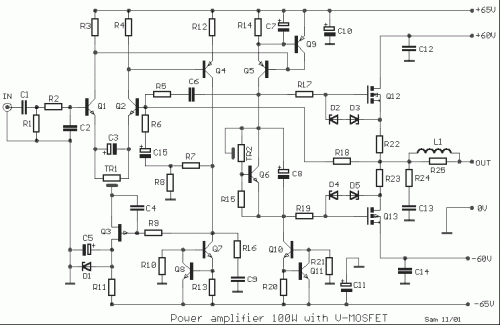
Power amp 100W with V-MosFet
Description
One still designing that it uses in the exit transistor of technology V-mosfet. This transistors to us offer a lot of virtues concerning the simple bipolar transistors, as high speeds, thermic stability, low distortion etc. Beyond this circuit use also other useful solutions as use fet as source of current [ Q3 ], trimmer TR1 with which we match the characteristics of differential amplifier of entry Q1-2. Also extensive is the use of sources of current wilson Q7-8 and Q10-11. With trimmer TR2 regulate the bias current of output stage, in the 100 ma. The use of diodes D2 until D5 in combination with the resistances R17-19, they protect the gates of transistors v-fet from exceeds the voltage ± 14V and it creates perforation in very thin layer SiO2, that is used as insulation in the gate. This way of protection is common in all the amplifiers that use these transistors. The total gain of amplifier is 32.6, regulated from the R18, R6 and R8, in the negative feedback. Also is used enough the use of local feedback for stabilisation of operation under all the conditions. Because the transistors v-fet have positive factor of temperature, with result with the increase of temperature is increased also their resistance. This increase has as result the reduction of current that via the transistor, hence also his power. The use of separated supply in the stages of drive and exit, ensures stability and reject of distortion of intermodulation. The initial drawing of is L. Hood and was published by the Wireless Word.
Circuit diagram
Part List
- R1=27Kohm
- R2-11=4.7Kohm
- R3-4=5.6Kohm
- R5=47Kohm
- R6=1Kohm
- R7-10-21=22Kohm
- R8=12ohm
- R9=1Mohm
- R12=33ohm
- R13-20=82ohm
- R14=33ohm
- R15=2.7Kohm
- R16=270ohm
- R17-19=680ohm
- R18=33Kohm
- R22-23=0.33ohm 5W
- R24=8.2ohm
- R25=10ohm 1W
- TR1=470ohm trimmer
- TR2=4.7Kohm trimmer
- C1=1uF 63V mkt
- C2=1nF 100V*
- C3=100uF 16V
- C4=100nF 100V*
- C5-7=22uF 16V
- C6=4.7pF ceramic
- C8=47uF 16V
- C9=1nF 100V*
- C10-11=100uF 100V
- C12-14=100nF 250V mkt
- C13=150nF 100V mkt
- C15=100uF 35V
- D1=12V 0.5W Zener
- D2.....5=8.2V 1W Zener
- L1=20 turns 0.6mm on R25
- Q1-2=BC 547
- Q3=2N5460 fet
- Q4-5=MPSA93
- Q6-8-11=BC182
- Q7-10=MPSA43
- Q9=BC212
- Q12=2SK134 or 2SK135
- Q13=2SJ49 or 2SJ50
*polyester or mylar
A branding that I want to make, that is in effect for all the amplifiers that I publish and use the POWER VMOS FET of series [ 2SK134 or 2SK135 ] [ 2SJ49 or 2SJ50 ], they are that, more above transistor they are not produced more by the Toshiba and are enough difficult they are found henceforth. They can be replaced with [ 2SK1530 in the place of 2SK135 ] and [ 2SJ201 in the place of 2SJ50 ]. The new transistors are in plastic case ΤΟ-3Ρ and no TO-3, bear in bigger supply of operation and have positive factor of temperature. This mean that with the increase of temperature, is increased and the current that is gone through from through the transistor. The new transistors him I have still not tryed and me it would interest to learn if somebody him used also with which results.
