- Hearing Aid
- Amplified Ear
- A Low Cost Hearing Aid
- Studio Series Stereo Headphone Amplifier
- Stereo Headphone Amplifier Circuit Schematic
- Pure Class-A Headphone Amplifier Schematic
- Portable Headphone Amplifier Circuit
- A Hiqh Quality Headphone Amplifier Schematic
- Ultra-High Fidelity High Power Amplifier Reference Design
- Speach Amplifier
- DC-Coupled Audio Amplifier
- A Low Power Wireless Audio Power Amplifier
- 8 Watt Audio Power Amplifier Schematic
- 7 Watt Audio Power Amplifier Circuit Schematic
- 60 Watt Audio Power Amplifier Circuit Diagram
45 Watt Class-B Audio Power Amplifier
Description
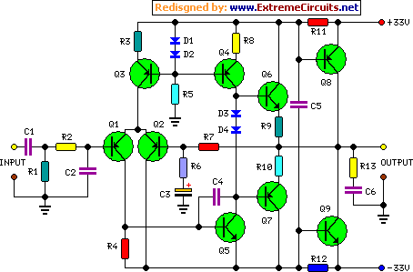
These goals were achieved by using a discrete-components op-amp driving a BJT complementary common-emitter output stage into Class B operation. In this way, for small output currents, the output transistors are turned off, and the op-amp provides all of the output current. At higher output currents, the power transistors conduct, and the contribution of the op-amp is limited to approximately 0.7/R11. The quiescent current of the op-amp biases the external transistors, and hence greatly reduces the range of crossover.
The idea sprang up from a letter published on Wireless World, December 1982, page 65 written by N. M. Allinson, then at the University of Keele, Staffordshire. In this letter, op-amp ICs were intended as drivers but, as supply voltages up to +/- 35V are required for an amplifier of about 50W, the use of an op-amp made of discrete-components was then considered and the choice proved rewarding.
The discrete-components op-amp is based on a Douglas Self design. Nevertheless, his circuit featured quite obviously a Class A output stage. As for proper operation of this amplifier a Class B output stage op-amp is required, the original circuit was modified accordingly. Using a mains transformer with a secondary winding rated at the common value of 25 + 25V (or 24 + 24V) and 100/120VA power, two amplifiers can be driven at 45W and 69W output power into 8 and 4 Ohms respectively, with very low distortion (less than 0.01% @ 1kHz and 20W into 8 Ohms).
This simple, straightforward but rugged circuit, though intended for any high quality audio application and, above all, to complete the recently started series of articles forming the Modular Preamplifier Control Center, is also well suited to make a very good Guitar or Bass amplifier. Enjoy!
Circuit diagram:
Parts:
- R1______________18K - 1/4W Resistor
- R2_______________3.9K - 1/4W Resistor
- R3,R6____________1K - 1/4W Resistors
- R4_______________2.2K - 1/4W Resistor
- R5______________15K - 1/4W Resistor
- R7______________22K - 1/4W Resistor
- R8_____________330R - 1/4W Resistor
- R9,R10__________10R - 1/4W Resistors
- R11,R12_________47R - 1/4W Resistors
- R13_____________10R - 1W Resistor
- C1_______________1µF - 63V Polyester Capacitor
- C2_____________470pF - 63V Polystyrene or Ceramic Capacitor
- C3______________47µF - 25V Electrolytic Capacitor
- C4______________15pF - 63V Polystyrene or Ceramic Capacitor
- C6_____________220nF - 100V Polyester Capacitor
- C6_____________100nF - 63V Polyester Capacitor
- D1,D2,D3,D4___1N4148 - 75V 150mA Diodes
- Q1,Q2________BC560C - 45V 100mA Low noise High gain PNP Transistors
- Q3,Q4________BC556 - 65V 100mA PNP Transistors
- Q5___________BC546 - 65V 100mA NPN Transistor
- Q6___________BD139 - 80V 1.5A NPN Transistor
- Q7___________BD140 - 80V 1.5A PNP Transistor
- Q8__________2N3055 - 60V 15A NPN Transistor
- Q9__________MJ2955 - 60V 15A PNP Transistor
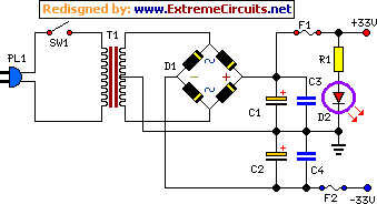
Power supply :
Parts:
- R1_______________3.3K - 1/2W Resistor
- C1,C2_________4700µF - 50V Electrolytic Capacitors
- C3,C4__________100nF - 63V Polyester Capacitors
- D1_____________200V 8A Diode bridge
- D2_____________5mm. Red LED
- F1,F2__________4A Fuses with sockets
- T1_____________230V or 115V Primary, 25+25V Secondary 120VA Mains transformer
- PL1____________Male Mains plug
- SW1____________SPST Mains switch
Comments:
The main design targets for this amplifier were as follows:
- Output power in the 40 - 70W range
- Simple circuitry
- Easy to locate, low cost components
- Rugged performance
- No setup
Notes:
- 2N3055 and MJ2955 transistors were listed for Q8 and Q9 as the preferred types, but many different output transistors can be used satisfactorily: TIP3055/TIP2955, TIP35/TIP36, MJ802/MJ4502 amongst others.
- Discrete op-amp output transistors Q6 and Q7 do not require any heatsink as their cases remain at ambient temperature. Power transistors Q8 and Q9 should be mounted on a black, finned heatsink as usual.
Technical data:
- Output power (1KHz sinewave): 45 Watt RMS into 8 Ohms - 69W RMS into 4 Ohms
- Sensitivity: 0.81V RMS input for 45W output
- Frequency response @ 1W RMS: 15Hz to 23KHz -0.2dB
- Total harmonic distortion @ 1KHz: 1W 0.008% 20W 0.008% 45W 0.016%
- Total harmonic distortion @10KHz: 1W 0.01% 20W 0.015% 45W 0.025%
- Unconditionally stable on capacitive loads
UPDATE
There is a little mistake in circuit diagram. Q8 and Q9 are displayed on wrong places. Please replace Q8's place wiht Q9's. Q8 is NPN Transistor 2N3055 and Q9 is MJ2955 PNP Transistor. Please update your notes.

